PowerEpi has successfully mastered the key technology for mass-producing high-quality SiC epitaxial wafers. The in-plane and inter-wafer uniformity of thickness and doping have reached first-class levels. Additionally, the defect control technology is on par with leading epitaxial manufacturers in the industry.
ince 2021, PowerEpi has successfully completed validation for its 4-inch 650V/10A SBD, 6-inch 650V/60mΩ MOSFET, 6-inch 1200V/30A SBD, and 6-inch 1200V/26mΩ MOSFET. The yield of these products is on par with industry-leading standards, and the quality of mass-produced units has received high acclaim from leading downstream device anufacturers.

Conventional Epiwafer
|
Items |
Standard |
Typical |
Standard |
|
|
Poly-type |
4H |
|||
|
Surface |
(0001) Si-face |
|||
|
Off-orientation |
4deg-off [11-20] |
|||
|
Conductivity |
n-type |
p-type |
||
|
Dopant |
Nitrogen |
Aluminum |
||
|
Carrier Concentration |
Range |
1E15~5E16 cm-3 |
1E15~5E16 cm-3 |
1E16 ~ 5E17 cm-3 |
|
Tolerance |
±10% |
±9% |
±20% |
|
|
Uniformity(s/mean) |
≤5% |
≤4% |
≤10% |
|
|
Epi thickness |
Range |
<20 μm |
<20 μm |
<20 μm |
|
Tolerance |
±6% |
±5% |
±6% |
|
|
Uniformity(s/mean) |
≤ 3% |
< 2% |
≤ 3% |
|
|
Surface defect |
≤0.6 cm-2 |
≤0.5 cm-2 |
≤0.6 cm-2 |
|
|
Surface roughness |
≤0.3 nm |
≤0.2 nm |
≤0.3 nm |
|
Notes:
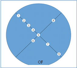
Measure points for Thickness and Carrier Concentration . Generally, the test method concludes 9 points (as shown in the figure), also the customer can assign the test method.

Ⅰ Carrier Concentration by Hg-CV.
Ⅱ Thickness by FTIR.
Ⅲ Surface defects include downfall, triangles, carrots, particles.
Ⅳ The roughness is tested by AFM, the scan size is 10×10μm2
Ⅴ Better products can be customized.

